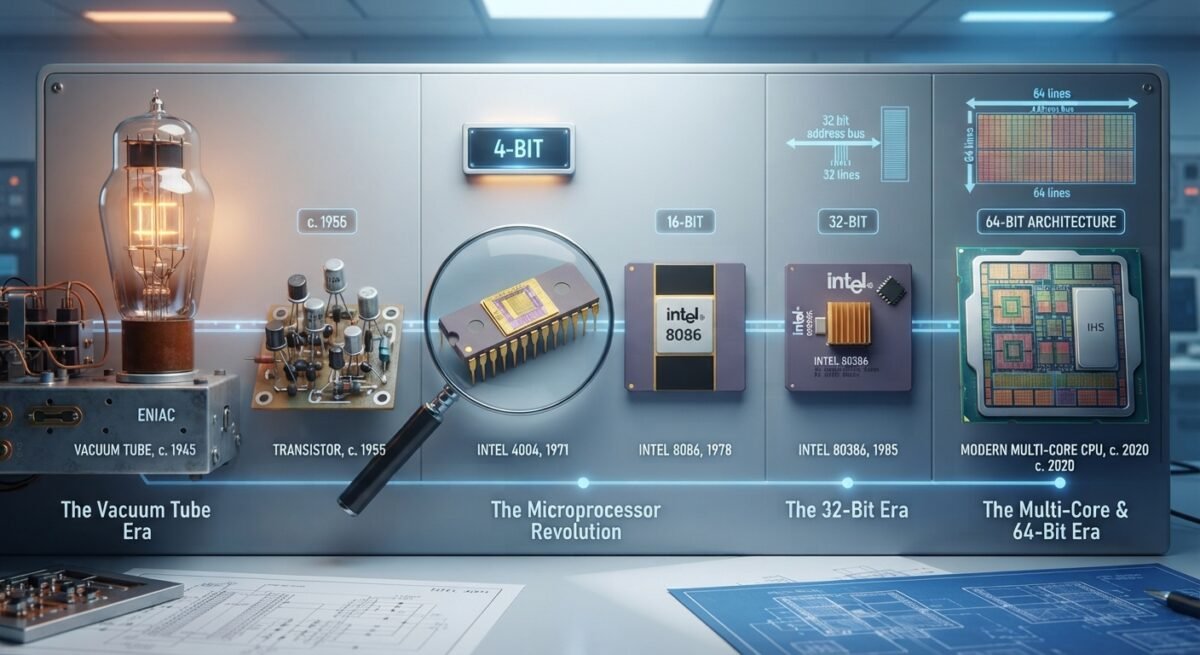
The Central Processing Unit (CPU) serves as the computational core of modern digital devices, executing program instructions through a continuous cycle of fetching, decoding, and executing data. Over the past eight decades, the CPU has evolved from room-sized assemblies of fragile glass vacuum tubes into microscopic silicon chips containing billions of transistors. This transformation—driven by breakthroughs in solid-state physics, architectural scaling, and the transition from 32-bit to 64-bit computing—redefined human industry, communication, and science.
The Vacuum Tube and Transistor Eras
In the mid-1940s, the earliest electronic computers relied on thousands of vacuum tubes to perform arithmetic and logic operations. Machines such as the ENIAC and the early UNIVAC systems occupied entire rooms, consumed massive amounts of electrical power, and generated enough heat to cause frequent tube burnouts. In these early systems, the processing unit was not a single component, but rather a sprawling collection of discrete cabinets wired together to implement the stored-program architecture conceptualized by John von Neumann.
The invention of the point-contact transistor at Bell Laboratories in 1947 inaugurated the second generation of computing. By replacing bulky vacuum tubes with solid-state semiconductor switches, engineers in the late 1950s and 1960s built CPUs that were dramatically smaller, faster, and more reliable. As companies like IBM automated transistor manufacturing, processing hardware transitioned from bespoke scientific instruments into commercial mainframes capable of handling enterprise data.
Integrated Circuits and the Microprocessor Revolution
A pivotal turning point arrived in 1958 and 1959, when Jack Kilby and Robert Noyce independently developed the integrated circuit (IC). Rather than wiring individual transistors together by hand, integrated circuits etched multiple transistors, resistors, and capacitors onto a single piece of semiconductor material. In 1965, Fairchild Semiconductor co-founder Gordon Moore observed that the number of components on an integrated circuit was doubling roughly every year—an observation later refined to every two years and immortalized as Moore’s Law.
By 1971, semiconductor density had advanced far enough to condense an entire CPU—including its arithmetic logic unit (ALU), control unit, and registers—onto a single chip. Developed by Ted Hoff, Federico Faggin, Masatoshi Shima, and Stanley Mazor, the Intel 4004 debuted as the world’s first commercially available microprocessor. Built using 10-micron silicon-gate technology, the 4-bit processor executed roughly 60,000 operations per second and democratized computing by making personal computers economically viable. Rapid succession followed with 8-bit chips like the Intel 8080 and 16-bit processors such as the Intel 8086, which established the foundational x86 instruction set architecture.
Scaling Bit Widths: The Leap from 32-Bit to 64-Bit
As software grew more sophisticated, processors evolved from 16-bit designs into 32-bit computing architectures, exemplified in the personal computer market by the Intel 80386 in 1985 and the Motorola 68000 family in workstations. A processor’s “bit width” defines the size of its internal registers, the amount of data it can process in a single operation, and the size of the memory addresses it can reference. A 32-bit CPU uses 32-bit memory pointers, allowing it to directly address 2^{32} bytes—or exactly 4 gigabytes (GB)—of random-access memory (RAM).
For nearly two decades, 4 GB of addressable memory was more than sufficient for mainstream desktops and operating systems. However, by the early 2000s, enterprise databases, scientific simulations, high-definition media editing, and virtualization began hitting the 4 GB ceiling. Overcoming this bottleneck required transitioning to 64-bit computing.
While pure 64-bit architectures had existed in specialized servers and workstations since the 1990s (such as DEC Alpha and IBM POWER3), the mainstream PC transition was catalyzed in 2003 when AMD introduced the Opteron and Athlon 64 processors utilizing x86-64 (also known as AMD64). Unlike competing clean-slate designs that struggled with legacy software, x86-64 extended the existing 32-bit x86 instruction set while maintaining native backward compatibility for 32-bit applications. Intel soon adopted compatible extensions under the Intel 64 banner, and ARM followed in 2011 with its 64-bit ARMv8-A architecture for mobile devices.
The architectural leap from 32-bit to 64-bit transformed CPU capabilities in three primary ways:
- Expanded Memory Addressing: A 64-bit address space expands theoretical memory limits from 2^{32} (4 GB) to 2^{64} bytes (16 exabytes), eliminating RAM bottlenecks for modern workloads.
- Wider and More Numerous Registers: In x86-64 mode, general-purpose registers doubled in width from 32 bits to 64 bits and doubled in count from 8 to 16, allowing the CPU to keep more active variables close to execution units and perform 64-bit integer arithmetic in a single clock cycle.
- Enhanced Hardware Security: Modern 64-bit architectures introduced hardware-enforced protections such as the No-Execute (NX) bit and stronger address space layout randomization, shielding operating systems from buffer-overflow exploits.
The Power Wall and the Multi-Core Era
For thirty years, CPU designers relied on Dennard scaling—a principle formulated by Robert Dennard in 1974—which observed that as transistors shrank, their voltage and current scaled down proportionally, keeping power density constant even as clock speeds climbed. This enabled single-core processors to race from megahertz into the gigahertz range during the 1990s and early 2000s.
Around 2005, Dennard scaling broke down. Transistors became so small that electrical current began leaking across atomic-scale barriers, causing chips to hit a thermal “power wall” where pushing clock speeds higher produced unmanageable heat. Rather than relying solely on faster single cores, chipmakers pivoted to multi-core architectures—placing two, four, eight, or dozens of independent processing cores onto a single silicon die to execute parallel threads simultaneously. Modern CPUs continue this trajectory through heterogeneous designs that combine high-performance cores, power-efficiency cores, and specialized neural engines onto tightly integrated systems-on-chip (SoCs).
Bibliography
- Computer History Museum. “Intel’s Microprocessor – CHM Revolution.” Computer History Museum Digital Logic Exhibit. Available at: https://www.computerhistory.org/revolution/digital-logic/12/285
- IBM. “The History of Central Processing Unit (CPU).” IBM Think Topics. Available at: https://www.ibm.com/think/topics/central-processing-unit-history
- IEEE Aerospace and Electronic Systems Society. “The History Column: Moore’s Law.” IEEE AESS. Available at: https://ieee-aess.org/post/blog/history-column-moores-law
- Wikipedia Contributors. “32-bit computing.” Wikipedia, The Free Encyclopedia. Available at: https://en.wikipedia.org/wiki/32-bit_computing
- Wikipedia Contributors. “64-bit computing.” Wikipedia, The Free Encyclopedia. Available at: https://en.wikipedia.org/wiki/64-bit_computing
- Wikipedia Contributors. “Central processing unit.” Wikipedia, The Free Encyclopedia. Available at: https://en.wikipedia.org/wiki/Central_processing_unit
- Wikipedia Contributors. “Dennard scaling.” Wikipedia, The Free Encyclopedia. Available at: https://en.wikipedia.org/wiki/Dennard_scaling
- Wikipedia Contributors. “Moore’s law.” Wikipedia, The Free Encyclopedia. Available at: https://en.wikipedia.org/wiki/Moore%27s_law
- Wikipedia Contributors. “x86.” Wikipedia, The Free Encyclopedia. Available at: https://en.wikipedia.org/wiki/X86
- Wikipedia Contributors. “x86-64.” Wikipedia, The Free Encyclopedia. Available at: https://en.wikipedia.org/wiki/X86-64
For a visual timeline summarizing how these processor generations evolved from the 1971 Intel 4004 to modern multi-core architectures, watch Evolution of CPU (1971–2026) | Intel, AMD, Nvidia & Apple Silicon.